Research programme

Fabrication of nano-devices using ultrafast lasers

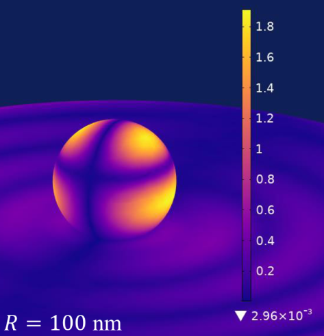
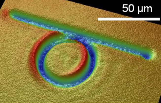
Integrated optics, having the unique properties of small size, low loss, high integration, and high scalability, is attracting considerable attention and has found many applications in optical communications, fulfilling the requirements for the ever-growing information rate and complexity in modern optical communication systems. Femtosecond laser fabrication is an acknowledged technique for producing integrated photonic devices with unique features, such as three-dimensional fabrication geometry, rapid prototyping, and single-step fabrication.

01

Laser induced periodic surface structures in silicon and diamond
pillars_and_lipss_edited.jpg

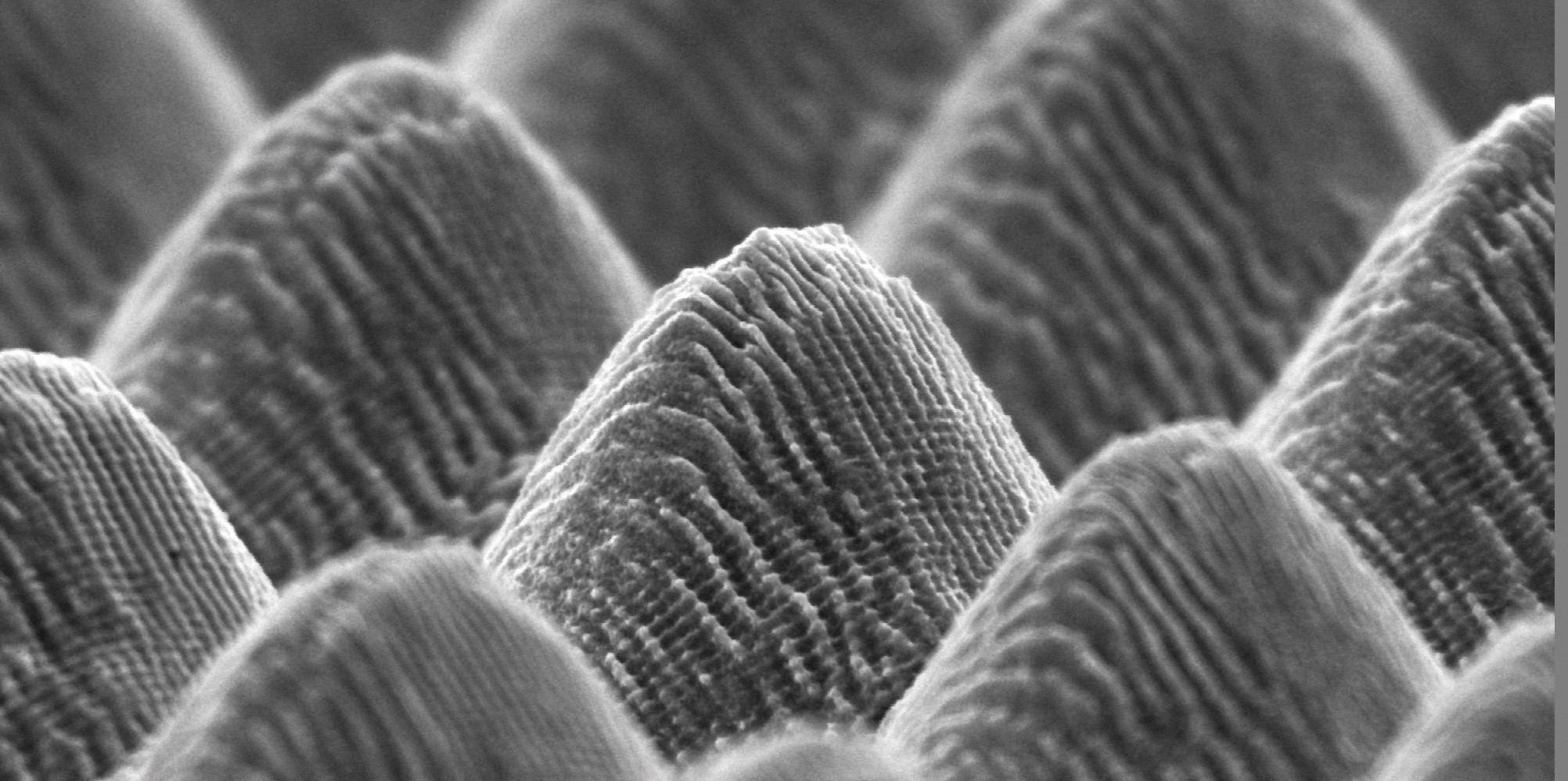
Laser-induced periodic surface structures (LIPSS, ripples) are a universal phenomenon that can be observed on almost any material after the irradiation by linearly polarized laser beams, particularly when using ultrashort laser pulses with durations in the picosecond to femtosecond range. During the past few years significantly increasing research activities have been reported in the field of LIPSS, since their generation in a single-step process provides a simple way of nanostructuring and surface functionalization towards the control of optical, mechanical or chemical properties.

Relevant publications in this area:

  • E. Granados* , M. Martinez-Calderon, B. Groussin, J. P. Colombier, I. Santiago, "Highly uniform silicon nanopatterning with deep-ultraviolet femtosecond pulses", Nanophotonics 13 (22), pp 4079-4089 (2024) [ PDF ]PDF
  • E. Granados* , M. M. Calderon, M. Gomez, A. Rodriguez, and S. M. Olaizola, "Photonic structures in diamond based on femtosecond UV laser induced periodic surface structuring (LIPSS)," Opt. Express 25, 15330-15335 (2017) [ PDF ]PDF
  • M. Martínez-Calderon, J. J. Azkona, N. Casquero, A. Rodríguez, Matthias Domke, M. Gómez-Aranzadi, S. M. Olaizola & E. Granados* , "Tailoring diamond’s optical properties via direct femtosecond laser nanostructuring", Scientific Reports 8, 14262 (2018) [ PDF ]PDF
  • E. Granados* , M. Martinez Calderon, J. Krzywinski, E. Wörner, A. Rodriguez, M. Gomez Aranzadi, and S. M. Olaizola, "Enhancement of surface area and wettability properties of boron doped diamond by femtosecond laser-induced periodic surface structuring," Opt. Mater. Express 7, 3389-3396 (2017) [ PDF]PDF]
02

Nanophotonics for electron emission

1_LIPSS2_edited.jpg

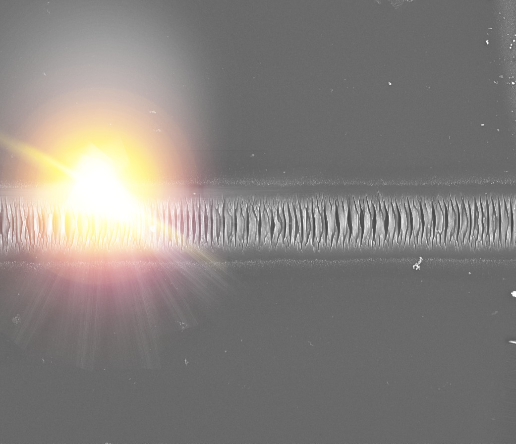
Finding new routes for enhancing the photo-emissive properties of materials without compromising their reliability is a crucial task. In this regard, plasmonic effects are poised to play a key role in the efficiency of photo-emissive devices. In the field of accelerator physics, plasmonic nanostructures enhancing non-linear and multi-photon photoemission from metallic nanoholes and nanogrooves have been demonstrated

There are significant advantages of operating in the linear photoemission regime while exploiting plasmonic effects; the lower intensity allows for higher charge production without material damage, while DUV laser technology currently could allow to operate at high average current. Here, in contrast to non-linear photoemission, the highly localized confinement of surface plasmons can lead to the production of high energy electrons via non-radiative decay, a process characterized by a significant deviation from the Fermi–Dirac distribution traditionally assumed in classic photoemission models. The combination of metallic nanostructures with ultra-thin-film dielectric coatings can further enhance the emission current density and corresponding QE of plasmonic nanostructures

  • M. Martinez-Calderon , B. Groussin , V. Bjelland , E. Chevallay , V. N. Fedosseev , M. Himmerlich , P. Lorenz , A. Manjavacas , B. A. Marsh , H. Neupert , R. E. Rossel , W. Wuensch and E. Granados* "Hot electron enhanced photoemission from laser fabricated plasmonic photocathodes," Nanophotonics (2023) [ PDF ]PDF
  • B. Groussin, M. Martinez-Calderon, O. Beldarrain, A. Rodriguez, Sa. M. Olaizola, B. A. Marsh, E. Granados* , "Efficient Composite Colorization of Copper by Spatially Controlled Oxidation with Deep-UV Ultrafast Lasers," Advanced Optical Materials 12, 2302071 (2024) [ PDF ]PDF
  • M. Martinez-Calderon, E. Chevallay, R. E. Rossel, L. B. Jones, G. Zevi Della Porta, B. Marsh, E. Granados* , "Fabrication and rejuvenation of high quantum efficiency caesium telluride photocathodes for high brightness and high average current photoinjectors," Phys. Rev. Acc. Beams 27, 023401 (2024) [ PDF]PDF]
03

Femtosecond UV etching for diamond photonics integrated circuits

nanophotonics.png

Diamond has long been recognized as an exceptional material featuring outstanding mechanical, thermal and optical properties. Beside these advantageous properties, an important stimulus that boosted researchers' interest in diamond photonics is the discovery of stable, room-temperature single photon emission from color centers hosted in single crystal diamond, as single photon sources are the enabling building block for a variety of quantum technologies in imaging, computing, and communication.

Although integrated photonic devices have been demonstrated in polycrystalline diamond, the performance in polycrystalline diamond will be inferior to single crystal diamond devices. For example, the propagation loss will be higher for polycrystalline diamond waveguides due to scattering at grain boundaries and increased surface roughness, and the grain boundaries in poly-diamond will lead to higher background noise in single photon sources. Here we show an alternative technique based on photo-oxidation processes on diamond surfaces at mesoscopic scales.

  • R. P. Mildren, J. E. Downes, J. D. Brown, B. F. Johnston, E. Granados , D. J. Spence, A. Lehmann, L. Weston, and A. Bramble, "Characteristics of 2-photon ultraviolet laser etching of diamond," Opt. Mater. Express 1, 576-585 (2011) [ PDF ]PDF
  • L. Weston, J. E. Downes, C. G. Baldwin, E. Granados , S. A. Tawfik, X. Y. Cui, C. Stampfl, and R. P. Mildren, "Photochemical Etching of Carbonyl Groups from a Carbon Matrix: The (001) Diamond Surface" Phys. Rev. Lett. 122, 016802 (2019) [ PDF ]PDF
  • E. Granados* , D. J. Spence, and R. P. Mildren, "Deep ultraviolet diamond Raman laser," Opt. Express 19, 10857-10863 (2011) [ PDF ]PDF
04

Photonic device fabrication and performance

etching_edited.jpg
  • J. J. Azkona, M. Martinez-Calderón, E. Granados , M. Gómez-Aranzadi, A. Rodriguez, and S. M. Olaizola, "Femtosecond laser fabrication of volume-phase gratings in CdSxSe1-x-doped borosilicate glass at a low repetition rate," Appl. Opt. 58, 4220-4226 (2019) [ PDF ]PDF
  • N Casquero, M. M.-Calderon, N. Perez, E. Granados , S. M. Olaizola and A. Rodriguez, "Polarization conversion on nanostructured metallic surfaces fabricated by LIPSS" LIMS Proceedings (2018) [ PDF ]PDF
  • A. San-Blas, M. Martinez-Calderon, E. Granados , M. Gómez-Aranzadi, A. Rodríguez, S.M. Olaizola, "LIPSS manufacturing with regularity control through laser wavefront curvature," Surfaces and Interfaces , Volume 25, 101205 (2021) [ PDF ]PDF
  • D. T. Echarri, A. San Blas, M. M. Calderon, S. Olaizola, E. Granados* , "Propagation of broadband coherent light through LIPSS-based metasurfaces in diamond" Opt. Mat. Express Vol. 12 No. 6 (2022)
  • E. Granados* "Development of highly efficient nanostructured metallic photocathodes fabricated by laser induced periodic surface structuring (LIPSS)" CERN Project Funded (2022)